 |
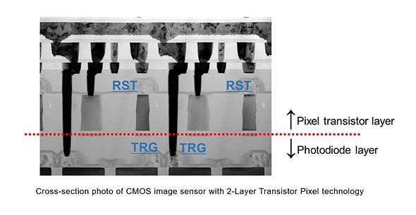
Sony Smiconductor Solutions Corporation (Sony) has announced it’s developed ‘the world’s first stacked CMOS image sensor technology with 2-Layer Transistor Pixel.’ This new technology separates the photodiodes from the pixel transistors onto different substrate layers, which nearly doubles the amount of light a single pixel can capture compared to more conventional image sensors.
Sony says its proprietary ‘2-Layer Transistor Pixel’ technology splits the photodiodes (which convert photons to electrical signals) and pixel transistors (which control those electrical signals) onto different layers of substrate stacked atop one another. In addition to optimized architectures, Sony says this stacked technology also enables them to increase the size of the amp transistors. These two benefits mean the individual pixels will have nearly double the saturation signal level and will be able to reduce the noise of images captured in low-light environment.
 |
| A comparison illustration showing how a conventional stacked CMOS sensor combines photo diodes and pixel transistors (left) compared to Sony’s new ‘2-Layer Transistor Pixel’ (right). |
Specifically, Sony says ‘The widened dynamic range and noise reduction available from this new technology will prevent underexposure and overexposure in settings with a combination of bright and dim illumination (e.g., backlit settings) and enable high-quality, low-noise images even in low-light (e.g., indoor, nighttime) settings.’
Sony doesn’t specify when we’ll see this inside consumer image sensors, but does suggest in the final sentence of its release that it’s designed with smartphone image sensors in mind.
